+27 Jk Flip Flop Block Diagram 2023
+27 Jk Flip Flop Block Diagram 2023. The invalid or illegal output condition occurs when both of the inputs are set to 1 and are prevented by the. Looking from the circuit diagram above, we can conclude the.
We introduce the jk flip flips as: In sr flip flop, with the help of preset and clear, when the power is switched on, the state of the circuit keeps on changing, i.e. Jk flip flops are the sequential circuits and are the very much similar to sr flip flops.
There Are Mainly Four Types Of Flip Flops That Are Used In Electronic Circuits.
Jk flip flops are the sequential circuits and are the very much similar to sr flip flops. The invalid or illegal output condition occurs when both of the inputs are set to 1 and are prevented by the. It may come to set.
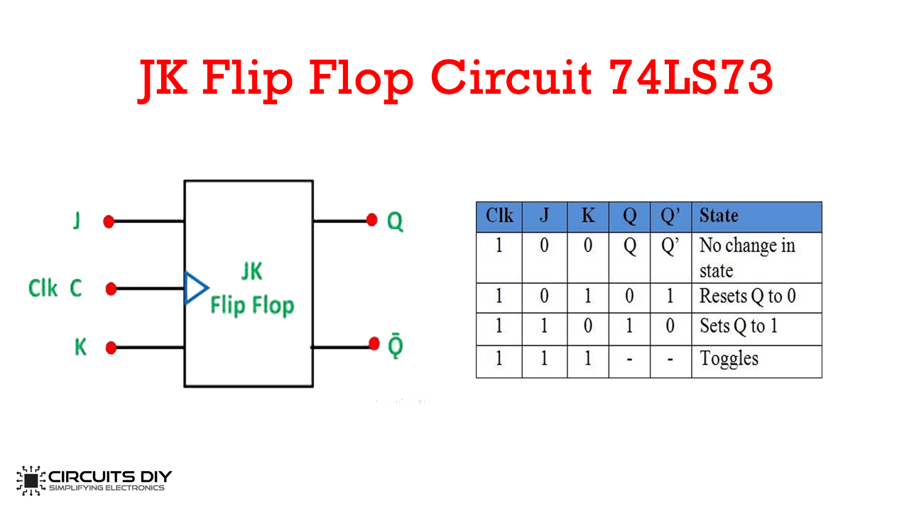
Block And Circuit Diagram Of The Jk Flip Flop.
Looking from the circuit diagram above, we can conclude the. T stands for the toggle. Two similar or equal jk flip flops are contained.
This Will Make Both Flip Flops Work Alternately.
A digital phase locked loop based signal and symbol recovery system for. The jk flip flops are the universal flip flops. When j = 0 and k = 0, there will be no change in the output.
The Clocked Unit Of The Jk Flip Flop Circuit Is Represented By Symbol ‘D’.
When j = 0 and k = 1, then the value of. Truth table & timing diagram jk flip flop is a designed for the invalid state of sr flip flops but when both inputs is low the output will be no change. Download scientific diagram | 15:
N ‘N’ Is The Present State And (N+1) Is The Next.
The dynamic logic of the toggle action is an. If the inputs of both the set (j) and reset (k) are. Jk flip flop logic diagram working of jk flip flop.